Nghiên cứu đặc trưng quang học của cấu trúc dị thể 2D MoS2/WS2 bằng phương pháp quang phổ ellipsometry
487 lượt xemDOI:
https://doi.org/10.54939/1859-1043.j.mst.101.2025.117-123Từ khóa:
Cấu trúc dị thể MoS2/WS2; Quang phổ ellipsometry; Mô hình Tauc-Lorentz; Đặc trưng quang học.Tóm tắt
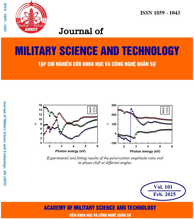
Nghiên cứu này xác định các đặc trưng quang học của cấu trúc dị thể 2D MoS2/WS2 bằng phép đo quang phổ ellipsometry (SE) trong dải phổ từ 1,5 đến 6,0 eV với các góc tới khác nhau. Các vật liệu kim loại chuyển tiếp chalcogenide như MoS2 và WS2, được biết đến với các tính chất đơn lớp độc đáo, rất lý tưởng cho các ứng dụng quang điện tử. Việc xếp chồng các lớp đơn này làm tăng cường các tính chất có lợi cho việc phát hiện ánh sáng và thu nhận ánh sáng. Phương pháp SE sử dụng mô hình Tauc-Lorentz để phân tích chi tiết, xác định sự hình thành của cấu trúc dị thể TMDC chất lượng cao và đưa ra chính xác các giá trị quan trọng về đặc trưng quang học của vật liệu bao gồm cả phần thực và phần ảo của chiết suất tại từng bước sóng trong khoảng 207 ~ 826 nm (tương đương với năng lượng photon 1,5 đến 6,0 eV). Các giá trị này rất quan trọng để tối ưu hóa các thiết bị quang điện tử dựa trên TMDC cho các ứng dụng quân sự và thương mại.
Tài liệu tham khảo
[1]. S. Manzeli, et al., “2D transition metal dichalcogenides”, Nature Reviews Materials, Vol. 2, No. 8, pp. 1-15, (2017). DOI: https://doi.org/10.1038/natrevmats.2017.33
[2]. A. Chaves, et al., “Bandgap engineering of two-dimensional semiconductor materials”, npj 2D Materials and Applications, Vol. 4, No. 1, pp. 29, (2020). DOI: https://doi.org/10.1038/s41699-020-00162-4
[3]. D. Monga, et al., “Advances in transition metal dichalcogenide-based two-dimensional nanomaterials”, Materials Today Chemistry, Vol. 19, No. pp. 100399, (2021). DOI: https://doi.org/10.1016/j.mtchem.2020.100399
[4]. M. Wu, et al., “Synthesis of two‐dimensional transition metal dichalcogenides for electronics and optoelectronics”, InfoMat, Vol. 3, No. 4, pp. 362-396, (2021). DOI: https://doi.org/10.1002/inf2.12161
[5]. X. Wu, et al., “Recent advances on transition metal dichalcogenides for electrochemical energy conversion”, Advanced Materials, Vol. 33, No. 38, pp. 2008376, (2021). DOI: https://doi.org/10.1002/adma.202008376
[6]. X. Wu, et al., “Recent Advances on tuning the interlayer coupling and properties in van Der Waals heterostructures”, Small, Vol. 18, No. 15, pp. 2105877, (2022). DOI: https://doi.org/10.1002/smll.202105877
[7]. M.S. Stark, et al., “Intercalation of layered materials from bulk to 2D”, Advanced Materials, Vol. 31, No. 27, pp. 1808213, (2019). DOI: https://doi.org/10.1002/adma.201808213
[8]. F. He, et al., “Moiré patterns in 2D materials: a review”, ACS nano, Vol. 15, No. 4, pp. 5944-5958, (2021). DOI: https://doi.org/10.1021/acsnano.0c10435
[9]. X. Guan, et al., “Recent progress in short‐to long‐wave infrared photodetection using 2D materials and heterostructures”, Advanced Optical Materials, Vol. 9, No. 4, pp. 2001708, (2021). DOI: https://doi.org/10.1002/adom.202001708
[10]. A. Elbanna, et al., “2D material infrared photonics and plasmonics”, ACS nano, Vol. 17, No. 5, pp. 4134-4179, (2023). DOI: https://doi.org/10.1021/acsnano.2c10705
[11]. H. Li, et al., “Recent progress and strategies in photodetectors based on 2D inorganic/organic heterostructures”, 2D Materials, Vol. 8, No. 1, pp. 012001, (2020). DOI: https://doi.org/10.1088/2053-1583/abbf04
[12]. Z. Yan, et al., “Emerging two‐dimensional tellurene and tellurides for broadband photodetectors”, Small, Vol. 18, No. 20, pp. 2200016, (2022). DOI: https://doi.org/10.1002/smll.202200016
[13]. X. Chen, C. Liu, and S. Mao, “Environmental analysis with 2D transition-metal dichalcogenide-based field-effect transistors”, Nano-micro letters, Vol. 12, No. pp. 1-24, (2020). DOI: https://doi.org/10.1007/s40820-020-00438-w
[14]. D. Tyagi, et al., “Recent advances in two-dimensional-material-based sensing technology toward health and environmental monitoring applications”, Nanoscale, Vol. 12, No. 6, pp. 3535-3559, (2020). DOI: https://doi.org/10.1039/C9NR10178K
[15]. M.S. Rahman and L.F. Abdulrazak, “Utilization of a phosphorene-graphene/TMDC heterostructure in a surface plasmon resonance-based fiber optic biosensor”, Photonics and Nanostructures-Fundamentals and Applications, Vol. 35, No. pp. 100711, (2019). DOI: https://doi.org/10.1016/j.photonics.2019.100711
[16]. K. Setayeshmehr, M. Hashemi, and N. Ansari, “Photoconversion efficiency in atomically thin TMDC-based heterostructures”, Opt. Express, Vol. 29, No. 21, pp. 32910-32921, (2021). DOI: https://doi.org/10.1364/OE.438386
[17]. Z. Hu, et al., “Interfacial charge and energy transfer in van der Waals heterojunctions”, InfoMat, Vol. 4, No. 3, pp. e12290, (2022). DOI: https://doi.org/10.1002/inf2.12290
[18]. I. Shahbaz, et al., “Advancements in 2D transition metal dichalcogenides (TMDs) inks for printed optoelectronics: A comprehensive review”, Materials Today, No., (2024). DOI: https://doi.org/10.1016/j.mattod.2024.06.008
[19]. C. Cong, et al., “Optical properties of 2D semiconductor WS2”, Advanced Optical Materials, Vol. 6, No. 1, pp. 1700767, (2018). DOI: https://doi.org/10.1002/adom.201700767
[20]. Y. Chen and M. Sun, “Two-dimensional WS 2/MoS 2 heterostructures: Properties and applications”, Nanoscale, Vol. 13, No. 11, pp. 5594-5619, (2021). DOI: https://doi.org/10.1039/D1NR00455G
[21]. R. Dutta, et al., “Optical Enhancement of Indirect Bandgap 2D Transition Metal Dichalcogenides for Multi‐Functional Optoelectronic Sensors”, Advanced Materials, Vol. 35, No. 46, pp. 2303272, (2023). DOI: https://doi.org/10.1002/adma.202303272
[22]. M. Wang, et al., “Manufacturing strategies for wafer-scale two-dimensional transition metal dichalcogenide heterolayers”, J. Mater. Res., Vol. 35, No. 11, pp. 1350-1368, (2020). DOI: https://doi.org/10.1557/jmr.2020.27
[23]. Y. Li, et al., “Measurement of the optical dielectric function of monolayer transition-metal dichalcogenides: MoS 2, Mo S e 2, WS 2, and WS e 2”, Physical Review B, Vol. 90, No. 20, pp. 205422, (2014).
[24]. X. Zhu, et al., “Effects of dielectric screening on the excitonic and critical points properties of WS 2/MoS 2 heterostructures”, Nanoscale, Vol. 12, No. 46, pp. 23732-23739, (2020). DOI: https://doi.org/10.1039/D0NR04591H
[25]. H.T. Nguyen, et al., “Temperature dependence of optical properties of monolayer WS2 by spectroscopic ellipsometry”, Applied Surface Science, Vol. 511, No. pp. 145503, (2020). DOI: https://doi.org/10.1016/j.apsusc.2020.145503
[26]. J. Humlíček, “Polarized light and ellipsometry”, in Handbook of ellipsometry. Springer. p. 3-91, (2005). DOI: https://doi.org/10.1016/B978-081551499-2.50003-4
[27]. R. Azzam, “Polarization, thin-film optics, ellipsometry, and polarimetry: Retrospective”, Journal of Vacuum Science & Technology B, Vol. 37, No. 6, (2019). DOI: https://doi.org/10.1116/1.5122802
[28]. B. Von Blanckenhagen, D. Tonova, J. Ullmann, “Application of the Tauc-Lorentz formulation to the interband absorption of optical coating materials”, Appl. Opt., Vol. 41, No. 16, pp. 3137-3141, (2002). DOI: https://doi.org/10.1364/AO.41.003137
[29]. L.V. Rodríguez-de Marcos, J.I. Larruquert, “Analytic optical-constant model derived from Tauc-Lorentz and Urbach tail”, Opt. Express, Vol. 24, No. 25, pp. 28561-28572, (2016). DOI: https://doi.org/10.1364/OE.24.028561
[30]. D.V. Likhachev, N. Malkova, and L. Poslavsky, “Modified Tauc–Lorentz dispersion model leading to a more accurate representation of absorption features below the bandgap”, Thin Solid Films, Vol. 589, No. pp. 844-851, (2015). DOI: https://doi.org/10.1016/j.tsf.2015.07.035
[31]. X. Ling, et al., “Parallel stitching of two-dimensional materials”, arXiv preprint arXiv:1512.04492, No. (2015).
[32]. J. Zhang, et al., “Observation of strong interlayer coupling in MoS2/WS2 heterostructures”, Advanced Materials, Vol. 28, No. 10, pp. 1950-1956, (2016). DOI: https://doi.org/10.1002/adma.201504631
[33]. S. Tongay, et al., “Tuning interlayer coupling in large-area heterostructures with CVD-grown MoS2 and WS2 monolayers”, Nano letters, Vol. 14, No. 6, pp. 3185-3190, (2014). DOI: https://doi.org/10.1021/nl500515q